-
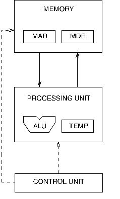
Communication between memory and processing unit consists of two registers:
-
Memory Address Register (MAR).
-
Memory Data Register (MDR).
-
-
To read,
-
The address of the location is put in MAR.
-
The memory is enabled for a read.
-
The value is put in MDR by the memory.
-
-
To write,
-
The address of the location is put in MAR.
-
The data is put in MDR.
-
The Write Enable signal is asserted.
-
The value in MDR is written to the location specified.
-
