-
Therefore, we can transform our results into a truth table, shown on the right.
-
Suddenly, this looks familiar:
-
The carry output is a simple AND function.
-
The sum is an XOR.
-
CIS-261 Home http://www.c-jump.com/bcc/c261c/CIS261syllabus.html
A key requirement of digital computers is the ability to use logical functions to perform arithmetic operations.
If we can add two binary numbers, then we should be able to:
subtract them, and
perform multiplication and division.
|
|
||||||||||||||||||||||||
|
|
Corresponding logic gate circuit, which adds inputs A and B, is known as half adder.
A half adder circuit has one significant drawback:
since pair of bits can produce an output carry,
in addition to the inputs A and B, we need to account for a possible carry over from a bit of the lower order of magnitude.
Unfortunately, half adder has no support for such carry over input by design.
Therefore, the combination requires not two, but three inputs to make the adder circuit more useful.
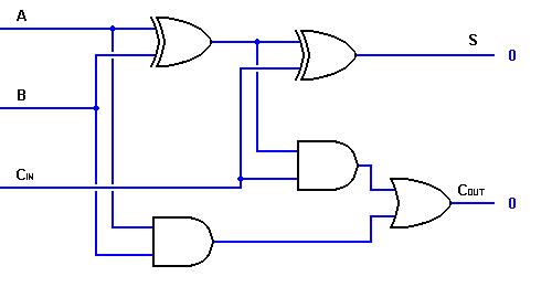
The circuit that does the entire job is called a full adder.
|
|
||||||||||||||||||||||||||||||||||||||||||||||||||
To implement the adder logic, we could combine two half-adder circuits together:

For the reasons explained later, we will examine a different version of the full adder circuit, as well as its functional details.
The second version of the full adder will have more primitive, brute force(*) implementation.
_____________
(*) Hacker Slang
|
|
|
|
|
|
For n rows we need 2n input AND-gates to construct the circuit.
For example, one-bit full adder had 3 inputs and required 8 = 23 input AND gates.
|
|
This kind of approach to implement the truth table implies the notion of being programmable.
We program our connections between the AND- and OR-gates while implementing desired logic functions.
Note that besides AND and OR the PLA may also include inverters.
We say that a set of gates
{AND, OR, NOT}
is logically complete, if we are able to:
draw a set of programmable connections between gates without any other kind of gate, and
completely satisfy the requirements of the truth table.
We may also say that such set of gates {AND, OR, NOT}
is sufficient to build an implementation of a given truth table, and
we don't need any other gates to do the job.