CIS-261 Home http://www.c-jump.com/bcc/c261c/CIS261syllabus.html

The Instruction Cycle


  1. The Instruction Cycle
  2. Fetch Instruction Phase
  3. Decode Instruction Phase
  4. Evaluate Operand Address Phase
  5. Fetch Operands Phase
  6. Steps in a Typical Read Cycle
  7. Execute phase
  8. Store Result Phase
  9. Steps in a Typical Write Cycle
  10. Properties of Memory
  11. ROM, Read-only Memory
  12. EPROM, Erasable PROMs
  13. RAM, Read/Write Memory
  14. DRAM Types
  15. Instruction Examples
  16. Changing the Sequence of Execution
  17. JMP Instruction Example
  18. Instruction Cycle FSM
  19. Micro-instructions and the Microcode
  20. Microcode Details
  21. Turing Machine
  22. Von-Neumann Machine Summary
  23. Von-Neumann Machine Cont.
  24. Von-Neumann Architecture Requirements

1. The Instruction Cycle


  • Instructions are processed under direction of the control unit in step-by-step manner.

  • Each step is referred to as a phase.

  • There are six fundamental phases of the instruction cycle:

    1. fetch instruction (aka pre-fetch)

    2. decode instruction

    3. evaluate address (address generation)

    4. fetch operands (read memory data)

    5. execute (ALU access)

    6. store result (writeback memory data)

  • Instruction cycle:

      Instruction cycle

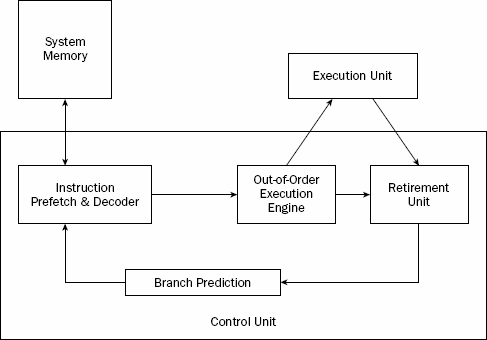
  • Pentium 4 instruction cycle:
      Pentium 4 instruction cycle

2. Fetch Instruction Phase


  • Obtain next instruction from memory.

  • Load instruction into instruction register IR.

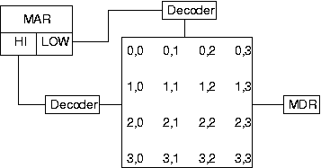
  • MAR is loaded with instruction pointer.

  • The instruction is loaded through the MDR.

  • Increment processor counter PC, that is, update instruction pointer address while reading instruction from memory.

  • Memory Circuitry:

      Memory Circuitry


  • Memory Operations:

      Understanding the MAR and the MDR

3. Decode Instruction Phase


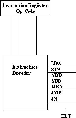
  • Decoder circuit examines opcode of the instruction.

  • Result is selecting unique decoder output line.

  • Output line signals a circuit which implements the corresponding operation.

  • Instruction decoder:

      Instruction decoder

4. Evaluate Operand Address Phase


  • Compute address of the memory location of the instruction operand.

  • Memory Circuitry:

      Memory Circuitry

5. Fetch Operands Phase


  • Load MAR with address calculated.

  • Read memory into MDR, making data available as input to the processing unit.

  • Memory Operations:

      Understanding the MAR and the MDR

6. Steps in a Typical Read Cycle


  1. Place the address of the location to be read on the address bus via MAR.

  2. Activate the memory read control signal on the control bus.

  3. Wait for the memory to retrieve the data from the addressed memory location.

  4. Read the data from the data bus into MDR.

  5. Drop the memory read control signal to terminate the read cycle.


7. Execute phase


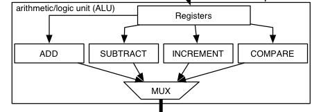
  • Microcode for the instruction, selected by the decoder output line, is executed by the ALU.

  • The ALU:

      ALU

8. Store Result Phase


  • Result is written to the designated destination of the instruction operand

  • Instruction Cycle begins anew.

  • Memory Operations:

      Understanding the MAR and the MDR

9. Steps in a Typical Write Cycle


  1. Place the address of the location to be written on the address bus via MAR.

  2. Place the data to be written on the data bus via MDR.

  3. Activate the memory write control signal on the control bus.

  4. Wait for the memory to store the data at the addressed location.

  5. Drop the memory write control signal to terminate the write cycle.


10. Properties of Memory


11. ROM, Read-only Memory


12. EPROM, Erasable PROMs


13. RAM, Read/Write Memory


14. DRAM Types


15. Instruction Examples


16. Changing the Sequence of Execution


17. JMP Instruction Example


18. Instruction Cycle FSM


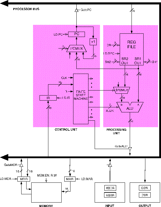
  • The diagram on the right shows a very abbreviated instruction cycle FSM of LC-3, the little computer.

  • Each state corresponds to one clock cycle.

  •   Instruction Cycle FSM of LC-3, little computer.

19. Micro-instructions and the Microcode


  • A computer program is executed as a series of individual CPU instructions.

  • CPU instructions constitute a machine-language level of abstraction.

  • Collections of logic circuits necessary to execute individual instructions are called microcode.

  • At the microcode level, there is a collection of programs that actually implement the instructions.

  • The micro-instructions are normally stored in permanent memory of the CPU itself.

  • LC-3, the little computer:

      LC-3, the little computer.

20. Microcode Details


21. Turing Machine


  • Turing machine is a mathematical model of a device that...

  • ...computes via a series of discrete steps, and

  • ...is not limited in use by a fixed amount of data storage.

    Universal Turing machine
  • The operations are limited to reading and writing symbols on an infinitely long tape.

  • At each step the machine reads the symbol at the current position on the tape.

22. Von-Neumann Machine Summary


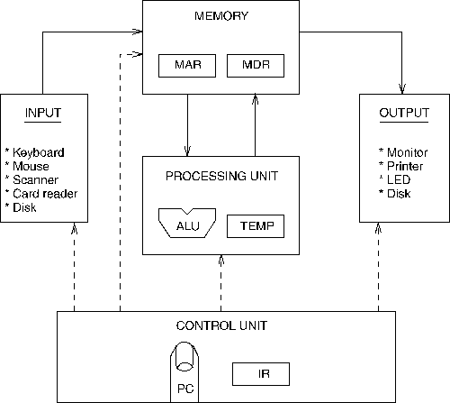
  • In contrast to a Turing machine, a von Neumann machine has a random-access memory (RAM) which means that each successive operation can read or write any memory location, independent of the location accessed by the previous operation.

  • The von Neumann Machine:

      The von Neumann Machine

  • A von Neumann machine also has a central processing unit (CPU) with one or more registers that hold data that are being operated on.

23. Von-Neumann Machine Cont.


  • The CPU has a set of built-in operations (its instruction set) that is far richer than with the Turing machine, including the arithmetic, logic, interrupt facilities, and memory access:

  • The CPU can interpret the contents of memory either as instructions or as data according to the fetch-execute cycle.

  • The von Neumann Machine:

      The von Neumann Machine

24. Von-Neumann Architecture Requirements


  1. Single stream of instructions, sequenced by instruction counter.

  2. Instructions stored with data in addressable memory.

  3. Instructions encoded as numbers and are modifiable by arithmetic operations.

  4. Radix 2 (binary) storage and math.

  5. Word length is long enough for scientific computation.

  6. Single address instructions, or single operand instructions, means that single, well-defined operations use exactly one memory address in combination with a register operand or immediate data.