CIS-261 Home http://www.c-jump.com/bcc/c261c/CIS261syllabus.html

Sequential Logic Circuits


  1. Sequential Logic Circuits
  2. Sequential Logic Circuits and FSM
  3. System State
  4. Finite State Machine, the FSM
  5. The State Diagram
  6. The State Diagram Example
  7. The Clock
  8. Traffic Danger Sign
  9. Danger Sign FSM
  10. Complete FSM example
  11. Complete FSM example, Cont.
  12. Combinational Logic Circuit
  13. Combinational Circuit Logic Gate Diagram
  14. Master-slave Flip-flop
  15. Master-slave Flip-flop, Cont.
  16. Additional Resources

1. Sequential Logic Circuits


  • Muxes, decoders, and full adders are combinational logic circuits.

  • Combinational logic circuits have no capacity of storing information.

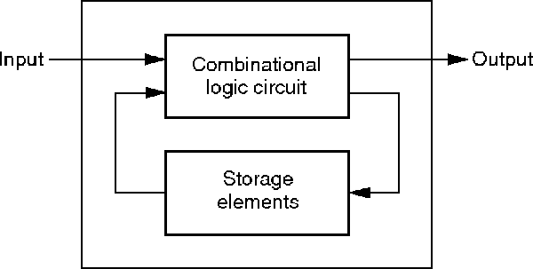
  • A different type, called sequential logic circuit, can, in addition to combinational logic, remember values and also base decisions on both input values and stored values.

  • Sequential logic circuit:

      Sequential logic circuit block diagram

2. Sequential Logic Circuits and FSM


  • Sequential logic circuits are building blocks of finite state machines.

  • Finite state machines are widely used.

  • For example, street traffic light controller device is FSM setting traffic lights to RGB values, depending on the combination of

    • current light setting, and

    • input from optical sensors on the road.


  • Sequential logic circuit:

      Sequential logic circuit block diagram

3. System State


  •   tic tac toe

  • The state of a system is a snapshot of all elements at the moment when the snapshot is taken.

  • For example, the progress of tic-tac-toe game can be described by snapshots of the board after each player's move.


4. Finite State Machine, the FSM


5. The State Diagram


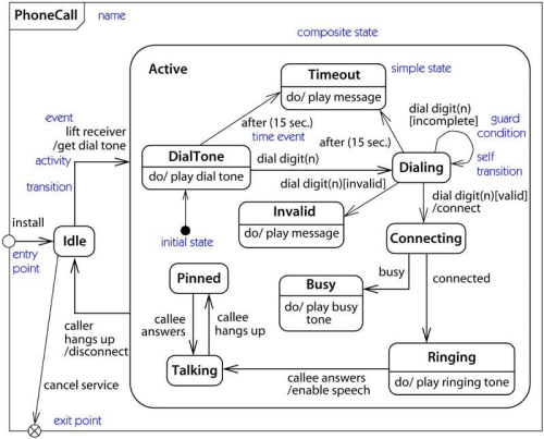
  • An FSM can be conveniently represented by means of the state diagram.

  • The states are represented by state symbols (rectangles with rounded corners or circles.)

  • The transitions are represented by arrows connecting the state symbols.

  • The state machine may be used as a protocol specification, showing the legal order of operations.

  • Phone call state UML diagram:

      phone call state diagram

6. The State Diagram Example


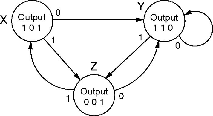
  • The output is 101 when system state is X.

  • The output is 110 when system state is Y.

  • The output is 001 when system state is Z.

  •   state diagram example

7. The Clock


  • How transitions from state to state are triggered? clock signal

  • A clock circuit is a mechanism that triggers FSM state transitions.

  • In digital logic terms, clock is a signal that alternates between 0 and 1.

  • The above picture shows repeated sequence of 3 signals, called clock cycles, or intervals.

  • In digital logic circuits, the transition from one FSM state to another occurs at the start of each clock cycle.

  • Clock cycle includes both 1 and 0 signals: 1 triggers transition, 0 allows to update internal information associated with the new state.

8. Traffic Danger Sign


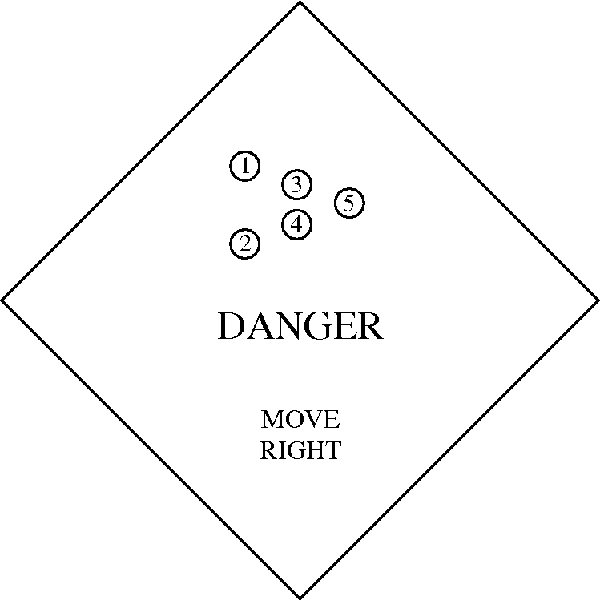
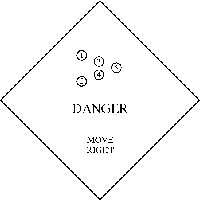
  • Consider traffic danger sign:

  •   danger sign

9. Danger Sign FSM


  •   danger sign

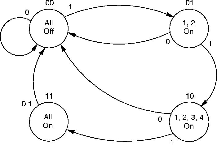
  • The purpose of FSM is to enable the lights to flash.

  • The FSM has one external switch: on/off.

  • Signals are visible on the diagram as 1 and 0 next to each state transition arrow.

  • Traffic danger sign FSM:

      danger sign FSM

10. Complete FSM example


  • The traffic danger sign can be in one of four states.

  • If external input is 0, we immediately transition to state named all off and remain in that state until external input changes back to 1.

  • If external input is 1, the lights should flash.

  •   danger sign FSM

11. Complete FSM example, Cont.


  • Light flash is implemented as external outputs unique to each state.

  • The FSM relies on two bits of memory to keep track of the lights behavior.

  • Thus, the FSM states are identified by four possible combinations of those two bits.

  •   danger sign FSM

12. Combinational Logic Circuit


13. Combinational Circuit Logic Gate Diagram


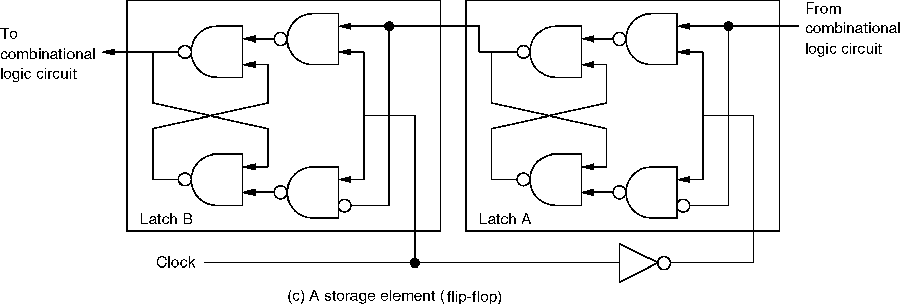
14. Master-slave Flip-flop


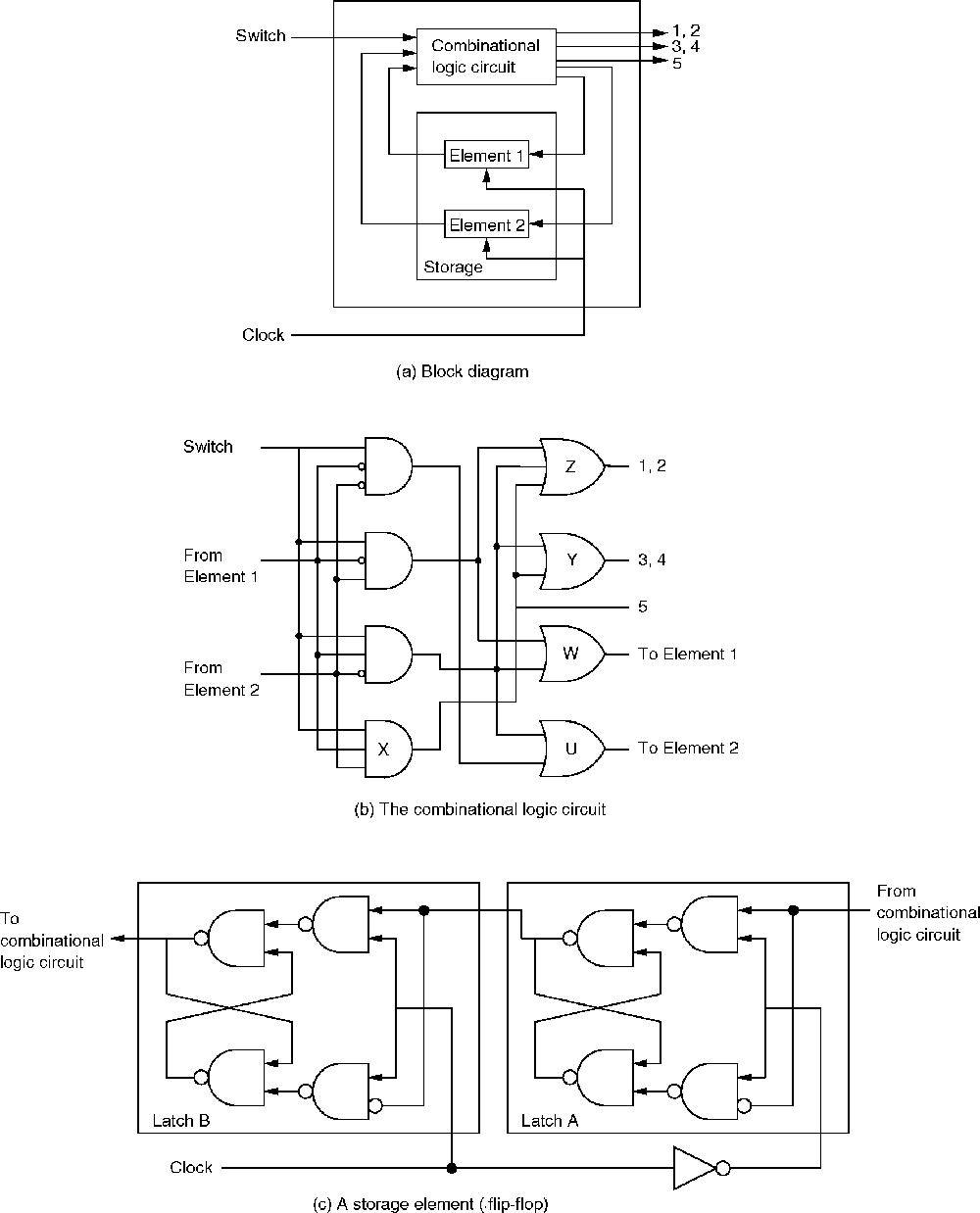
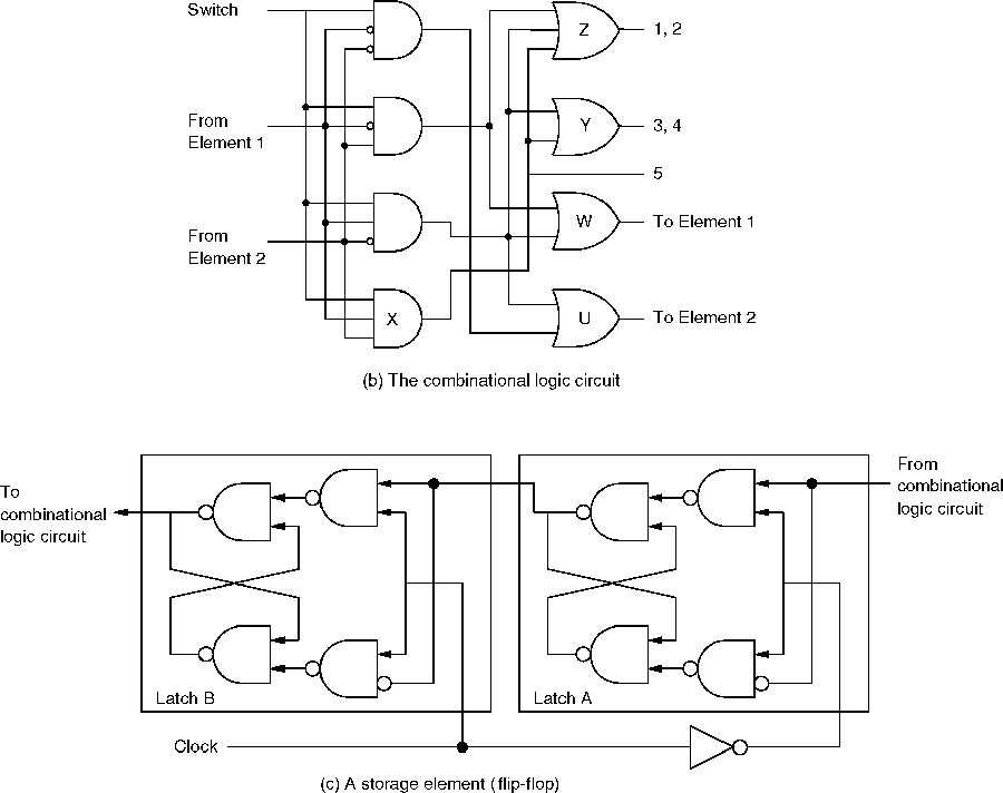
  • Half 1, clock signal is 1:

    1. Latch A value is protected.

    2. Latch A value is passed to latch B.

    3. Latch B value becomes input to the logic circuit.

  • Half 2, clock signal is 0:

    1. Latch B value becomes protected.

    2. Latch A becomes enabled for writing and accepts the output of the logical circuit.

15. Master-slave Flip-flop, Cont.


16. Additional Resources