CIS-261 Home http://www.c-jump.com/bcc/c261c/CIS261syllabus.html

Storage Elements


  1. Basic Storage Elements
  2. The R-S Latch
  3. The R-S Latch, Cont.
  4. The R-S Latch Set Example
  5. The R-S Latch Design Requirements
  6. The Gated D Latch
  7. The Gated D Latch, Cont.
  8. A Register
  9. Bit Sequences
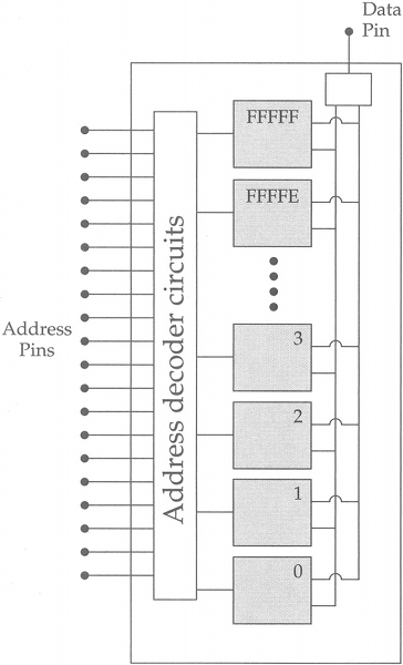
  10. The Concept of Memory
  11. Address Space
  12. Addressability
  13. A 22-by-3 Bit Memory
  14. A 22-by-3 Bit Memory, Cont.
  15. Reading Memory Location Example
  16. Writing Memory

1. Basic Storage Elements


2. The R-S Latch


  • The R-S latch can store one bit of information.

  • Also known as the Basic RS NAND Latch.

  • It works as follows:

  • The inputs are generally designated "S" and "R" for "Set" and "Reset", respectively.

  • Assume that S=1 and R=1.

  • If a=1, then A=1 and b=0 and B=0 and a=1.

  • R-S latch circuit: R-S latch

3. The R-S Latch, Cont.


  • If a=0, then A=0 and b=1 and B=1 (and a=0 because S=1.)

  • Again, as long as S=1 and R=1, the state of the circuit will not change:

    • R-S latch stores the value 0 , which corresponds to the value of output a=0.

  • If we set S=0 while R=1, the latch will be set to 1.

  • If we set R=0 while S=1, the latch will be set to 0.

  • R-S latch circuit: R-S latch

4. The R-S Latch Set Example


  • To set the latch, we need to momentarily set S=0, and then flip it back to S=1.

  • If we clear S, then a=1, and A=1.

  • Since R=1, b=0. This makes B=0, which makes a=1.

  • If we restore S=1, a will not change, because B=0.

  • Therefore, the latch continues to store value 1 as long as S=1.

    (In a similar way, we can clear the latch by momentarily setting R=0 and back to R=1.)

  •   R-S latch

5. The R-S Latch Design Requirements


  • The latch must never be supplied S=0 and R=0 at the same time:

    • Cleared S=0 and R=0 at the same time are forbidden inputs.

  • If this happens, subsequent latch value will be undefined.

  • Applying a sequence of logic 0 to the same gate has no effect on the state of the circuit.

  • Only applying a logic 0 to the other gate will cause the latch state change.

  •   R-S latch

6. The Gated D Latch


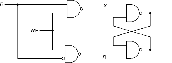
  • D stands for the Data latch, or D-latch, as it is generally called.

  • The gated D-latch consists of

    • one R-S latch, and

    • two additional gates, which allow the latch to be set equal to the value of D, but only when WE is asserted (set to 1).

  •   Gated D Latch

7. The Gated D Latch, Cont.


  • WE input is typically designated as clock input, since it is often controlled by a clock circuit that synchronizes several latch circuits with each other.

  • The output can only change state while clock input is 1.

  • When clock is 0, the S and R inputs have no effect.

  • See also: D NAND latch

  •   Gated D Latch

  • If WE is momentarily asserted, (set to 1), either R or S will be set to 0, depending on the current value of D:

    • if D=1, then S=0, causing the latch to change to 1.

    • if D=0, then R=0, causing the latch to change to 0.

  • Once WE returns to 0, both S and R return to 1, and the value stored in the latch will persist.

8. A Register


  • The register is a structure that stores a number of bits as one unit.

  • Register size determines the number of stored bits.

  • Number of bits caw range from 1 to the necessary size.

  • A four-bit register:

      four-bit register

9. Bit Sequences


10. The Concept of Memory


11. Address Space


12. Addressability


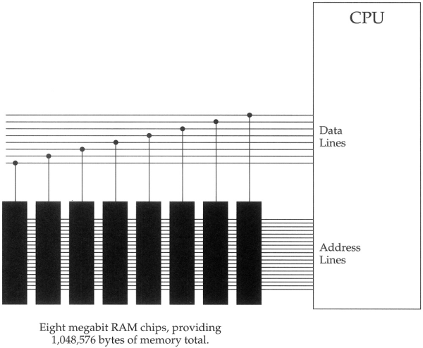
  • The number of bits stored at each memory location is characterized as addressability.

  • Most memories are byte-addressable.

  • Many computers today are 64-bit -addressable, allowing manipulation of 64-bit floating point numbers.

  •   CPU and memory

13. A 22-by-3 Bit Memory


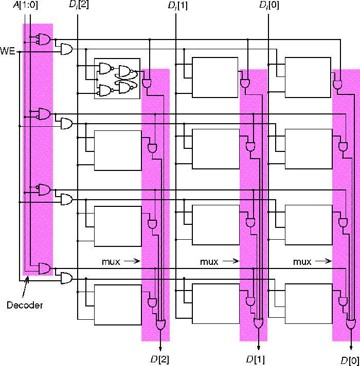
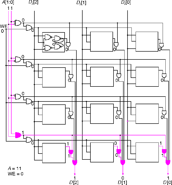
  • Memory of size 22-by-3 bit is made of 4-row by 3-column array of D-latches.

  • Address space is 22, which allows access to four unique memory locations.

  • Each memory location is shown horizontally.

  • Addressability is 3 bits, which allows storage of 3 bits in each location.

  • There are two address bits, shown as A[1:0]

  •   4-by-3 bit memory

14. A 22-by-3 Bit Memory, Cont.


  • Decoder takes A[1:0] and asserts exactly one of its four outputs, pointing to a row of memory.

  • Each memory location yields a unique three-bit word.

  • Horizontal locations for data input and output are called word lines.

  • Entire circuit is a mux of output signals with built-in decoder for selection of data values.


  •   4-by-3 bit memory

15. Reading Memory Location Example


  1. The binary code for 3 is 11.

  2. Address A[1:0] = 11 is decoded, and the bottom word line is asserted.

  3. The value stored in memory location 3 is equal to 101.

  4. All output lines are ANDed and subsequently ORed to produce the D[2:0]=101 result.

  • RAM chip diagram: A RAM chip

  •   Reading 4-by-3 bit memory

16. Writing Memory


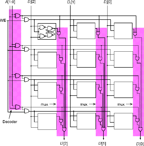
  • Writing memory is similar to reading:

    1. address is presented to the decoder

    2. correct word line is asserted

    3. WE is asserted as well

    4. bits Di[2:0] are written into the three gated D-latch that corresponds to the selected horizontal word line.

  •   Reading 4-by-3 bit memory