CIS-261 Home http://www.c-jump.com/bcc/

The von Neumann Computer Model


  1. The von Neumann Computer Model
  2. Components of the Von Neumann Model
  3. Communication Between Memory and Processing Unit
  4. CPU data-path
  5. Memory Operations
  6. Understanding the MAR and the MDR
  7. Understanding the MAR and the MDR, Cont.
  8. ALU, the Processing Unit
  9. ALU and the Word Length
  10. Control Unit
  11. Control Unit, Cont.
  12. Input/Output
  13. Input/Output Ports
  14. Input/Output Address Space
  15. Console Input/Output in Protected Memory Mode
  16. Instruction Processing
  17. Instruction Components
  18. Why Learn Intel x86 ISA ?
  19. Design of the x86 CPU Instruction Set
  20. CPU Instruction Set
  21. History of IBM PC
  22. Early x86 Processor Family
  23. 8086 and 8088 CPU
  24. 80186 CPU
  25. 80286 CPU
  26. 80386 CPU
  27. 80386 CPU, Cont.
  28. 80486 CPU
  29. Pentium (Intel 80586)
  30. Pentium Pro
  31. Pentium II
  32. Itanium processor

1. The von Neumann Computer Model


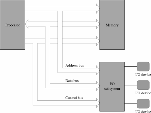
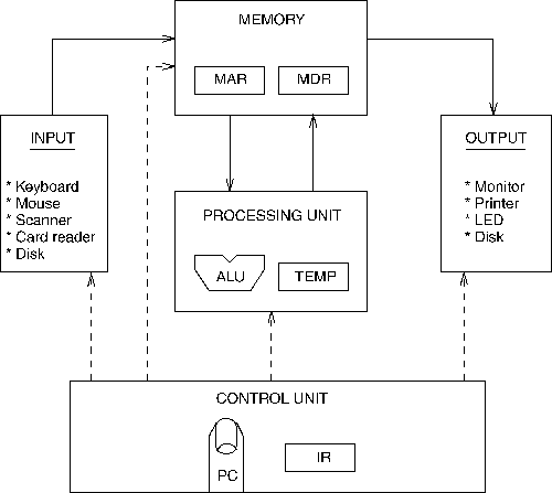
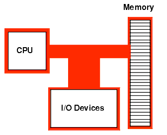
  • Von Neumann computer systems contain three main building blocks:

    • the central processing unit (CPU),
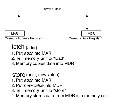
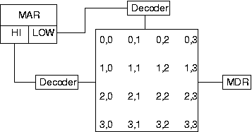
    • memory,

    • and input/output devices (I/O).

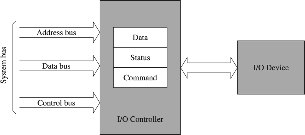
  • These three components are connected together using the system bus.

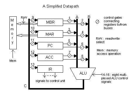
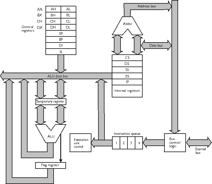
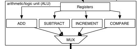
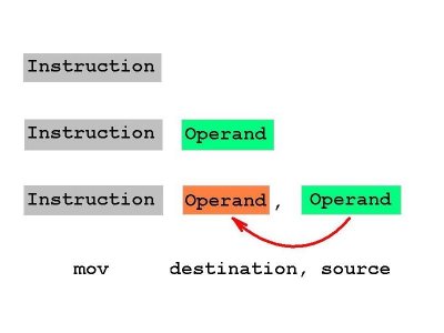
  • The most prominent items within the CPU are the registers: they can be manipulated directly by a computer program.

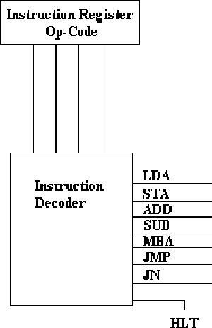
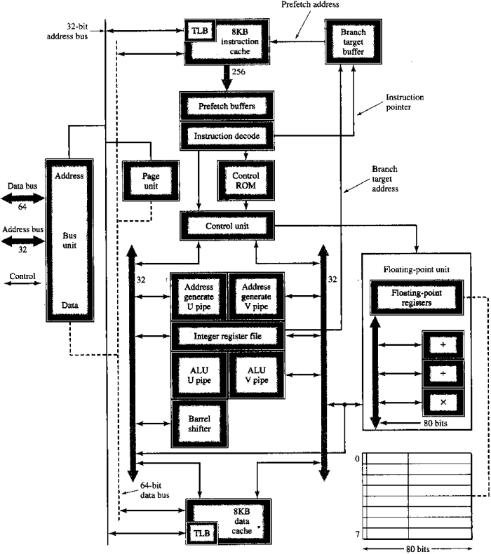
  • The following block diagram shows major relationship between CPU components:

      Simplified view of computer system

2. Components of the Von Neumann Model


  1. Memory: Storage of information (data/program)

  2. Processing Unit: Computation/Processing of Information

  3. Input: Means of getting information into the computer. e.g. keyboard, mouse

  4. Output: Means of getting information out of the computer. e.g. printer, monitor

  5. Control Unit: Makes sure that all the other parts perform their tasks correctly and at the correct time.

  • The von Neumann Machine:

      The von Neumann Machine

3. Communication Between Memory and Processing Unit


  • Communication between memory and processing unit consists of two registers:

    • Memory Address Register (MAR).

    • Memory Data Register (MDR).

  • To read,

    1. The address of the location is put in MAR.

    2. The memory is enabled for a read.

    3. The value is put in MDR by the memory.

  • To write,

    1. The address of the location is put in MAR.

    2. The data is put in MDR.

    3. The Write Enable signal is asserted.

    4. The value in MDR is written to the location specified.

  •  

      The von Neumann Machine

4. CPU data-path


  • Hardware units like ALU's, registers, memory, etc., are linked together into a data-path.

  • The flow of bits around the data-path is controlled by the "gates" which allow the bits to flow (on) or not flow (off) through the data-path.

  • The binary instructions (1 = on; 0 = off) that control the flow are called micro-instructions.

  •   CPU data-path

5. Memory Operations


  • There are two key operations on memory:

    1. fetch( address ) returns value without changing the value stored at that address.

    2. store( address, value ) writes new value into the cell at the given address.

  • This type of memory is random-access, meaning that CPU can access any value of the array at any time (vs. sequential access, like on a tape).

  • Such memories are called RAM (random-access memory.)

  • Some memory is non-volatile, or read-only (ROM or read-only memory.)


  • Memory Operations:

      Understanding the MAR and the MDR

6. Understanding the MAR and the MDR


  • MAR stands for memory address register:

    • MAR is connected to the address bus.

    • MAR is "the only way" for the CPU to communicate with address bus.

    • Tri-state buffer between MAR and the address bus prevents MAR from continously dumping its output to the address bus.

    • MAR can hold either an instruction address or a data address.


  • Memory Circuitry:

      Understanding the MAR and the MDR

7. Understanding the MAR and the MDR, Cont.


  • MDR Stands for memory data register.

    • MDR is connected to the data bus.

    • Data can go in both directions: to and from memory,

      • therefore, MDR can load its data from

        • the data bus (for reading data)

        • one of the CPU registers (for storing data.)

    • A 2-1 MUX circuit selects input from one of the two.

  • Memory Circuitry:

      Understanding the MAR and the MDR

8. ALU, the Processing Unit


  • Processing unit is hardware that implements Arithmetic and Logical Operations.

  • ALU stands for Arithmetic and Logic Unit, capable of performing

            ADD, SUBTRACT, AND, OR, and NOT
    

    operations.

  • The ALU:

      x86 data path

9. ALU and the Word Length


10. Control Unit


  • Manages the Precessing Unit.

  • Implemented as FSM.

  • FSM directs all activity.

  • Clock-based step-by-step precessing, cycle-by-cycle.

  • FSM is controlled by the

    1. Clock signal

    2. Instruction Register

    3. Reset signal

  •   The von Neumann Machine

11. Control Unit, Cont.


  • Control unit includes

    • Instruction Register IR

    • Instruction Pointier IP (aka Program Counter PC)

  • FSM outputs of the control unit,

        - - - - ->
    

    shown by dash lines, have two purposes:

    1. Control processing that takes place inside the ALU.

    2. Authorize read/write gate control of the CPU data-path.

  •   The von Neumann Machine

12. Input/Output


13. Input/Output Ports


14. Input/Output Address Space


15. Console Input/Output in Protected Memory Mode


  • Using console in Protected Memory Mode:

    • Keyboard input

    • Console display output

    • Ascii character encoding

  • Von Neumann Computer System Block Diagram:

      Von Neumann Computer System Block Diagram

16. Instruction Processing


17. Instruction Components


  • Instruction in memory has two parts: opcode and operands.

  • The opcode identifies the operation that instruction does

  • The operands are subjects of the operation, such as data values, registers, or memory addresses.

  • Due to variety of opcodes and operands, instructions may occupy different sizes of bytes in memory.

  • Instructions with no operands can have implied operands, those that are not explicitly shown.

  • Instruction formats:

      Instruction formats

18. Why Learn Intel x86 ISA ?


19. Design of the x86 CPU Instruction Set


20. CPU Instruction Set


  • A typical Von Neumann architecture encodes CPU instructions as numeric values in memory.

  • Programming and engineering of the instruction set is a major task in the CPU design.

  • Each instruction needs a unique numeric opcode.

  • Instruction formats:

      Instruction formats


  • Instruction decoder:

      Instruction decoder

21. History of IBM PC


22. Early x86 Processor Family


23. 8086 and 8088 CPU


  • Year 1979

  • The 8088, 8086, and 80286 are 16-bit CPUs.

  • Internal registers are 16 bits in size.

  • The 8086 is faster than the 8088 because of its 16-bit data bus; the 8088 has only an 8-bit data bus.

  • The 16-bit data bus allows you to use EVEN and ALIGN on an 8086 processor to word-align data and thus improve data-handling efficiency.

  • Memory addresses on the 8086 and 8088 refer to actual physical addresses.

  • The 8086 and 8088 have 20 address pins, and 1 megabyte of addressable memory (which is the real mode segmented memory explained later) requires addresses of 20 bits in size.

  • See also: Brief History of Microprocessors

  •   Structure 8086

24. 80186 CPU


25. 80286 CPU


26. 80386 CPU


27. 80386 CPU, Cont.


28. 80486 CPU


29. Pentium (Intel 80586)


30. Pentium Pro


31. Pentium II


32. Itanium processor