10-3
INPUT/OUTPUT
All the IA processors that have on-chip caches also provide the PCD (page-level cache disable)
flag in page table and page directory entries. This flag allows caching to be disabled on a page-
by-page basis. Refer to Chapter 3.6.4., Page-Directory and Page-Table Entries in Chapter 3,
Protected-Mode Memory Management, in the Intel Architecture Software Developers Manual,
Volume 3.
10.4.I/O INSTRUCTIONS
The processors I/O instructions provide access to I/O ports through the I/O address space.
(These instructions cannot be used to access memory-mapped I/O ports.) There are two groups
of I/O instructions:
Those which transfer a single item (byte, word, or doubleword) between an I/O port and a
general-purpose register.
Those which transfer strings of items (strings of bytes, words, or doublewords) between an
I/O port and memory.
The register I/O instructions IN (input from I/O port) and OUT (output to I/O port) move data
between I/O ports and the EAX register (32-bit I/O), the AX register (16-bit I/O), or the AL
(8-bit I/O) register. The address of the I/O port can be given with an immediate value or a value
in the DX register.
The string I/O instructions INS (input string from I/O port) and OUTS (output string to I/O port)
move data between an I/O port and a memory location. The address of the I/O port being
accesses is given in the DX register; the source or destination memory address is given in the
DS:ESI or ES:EDI register, respectively.
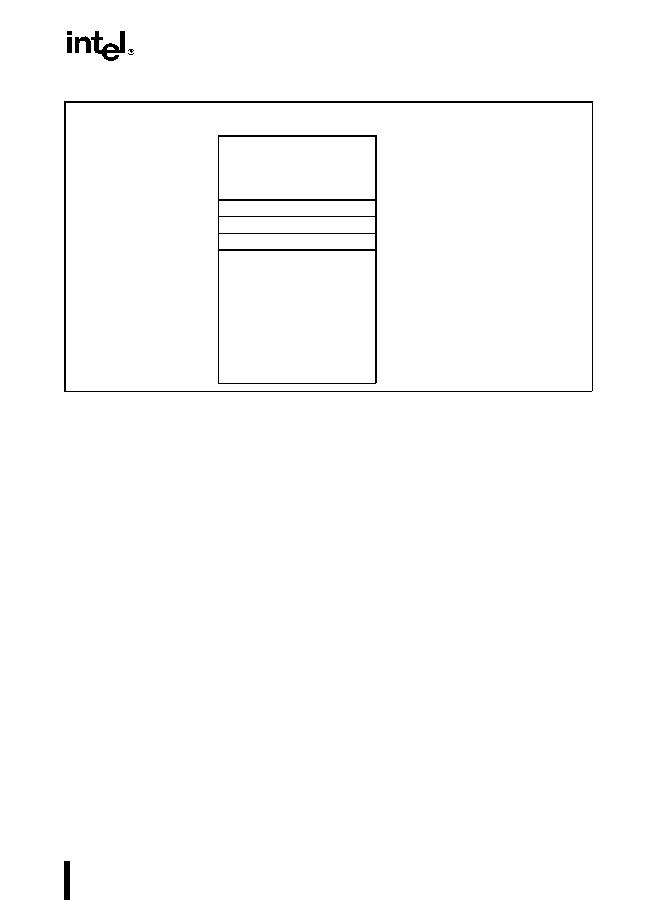
Figure 10-1. Memory-Mapped I/O
FFFF FFFFH
I/O Port
EPROM
RAM
Physical Memory
0
I/O Port
I/O Port

