<<< Combinational Circuit Logic Gate Diagram     Index     Pulse Triggered Flip-flop, Cont. >>>

14. Pulse Triggered Flip-flop


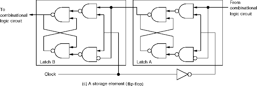
  • Half 1, clock signal is 1:

    1. Latch A value is protected.

    2. Latch A value is passed to latch B.

    3. Latch B value becomes input to the logic circuit.

  • Half 2, clock signal is 0:

    1. Latch B value becomes protected.

    2. Latch A becomes enabled for writing and accepts the output of the logical circuit.

<<< Combinational Circuit Logic Gate Diagram     Index     Pulse Triggered Flip-flop, Cont. >>>